HVPE Gallium Nitride GaN Wafer , Gan Chip Free Standing 10 x 10 mm Size
1. What is GaN substratesGallium Nitride is one kind of wide-gap compound semiconductors. It is made with original HVPE method and wafer processing technology, which has been originally developed for many years.
2.Application
Laser diodes for Blu-ray Disc™ players and light projectors
Future application: GaN PN-diode with high breakdown voltage over 3,000V and low on-resistance of 1mΩ·cm2
long-lived, efficient and reliable optoelectronic and electronic devices
high brightness LEDs for general lighting and high power, high frequency transistors for cellular phone base stations and defence applications.
3.Product available
2"GaN substrates
small pieces (10*10.5mm) for your testing usage
GaN-template with highly doped n-type layer (n=<1e19/cm3)
Ntype (undoped), Ntype (Ge doped), and Semi-insulating(Fe doped) substrates are available
Non-polar and semi-polar GaN substrates
4. Features
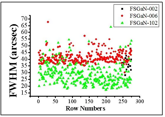
high crystalline, good uniformity, and superior surface quality
| XRD-FWHM | 002 | 102 |
| 350μm FSGaN | 25-45 | 20-55 |
5. Specification
| Item | GaN-FS-C-U-C50 | GaN-FS-C-N-C50 | GaN-FS-C-SI-C50 |
| Dimensions | Ф 50.8 mm ± 1 mm | ||
| Thickness | 350 ± 25 µm | ||
| Useable Surface Area | > 90% | ||
| Orientation | C-plane (0001) off angle toward M-Axis 0.35°± 0.15° | ||
| Orientation Flat | (1-100) ± 0.5°, 16.0 ± 1.0 mm | ||
| Secondary Orientation Flat | (11-20) ± 3°, 8.0 ± 1.0 mm | ||
| TTV (Total Thickness Variation) | ≤ 15 µm | ||
| BOW | ≤ 20 µm | ||
| Conduction Type | N-type (Undoped) | N-type (Ge-doped) | Semi-Insulating (Fe-doped) |
| Resistivity(300K | < 0.5 Ω·cm | < 0.05 Ω·cm | >106 Ω·cm |
| Dislocation Density | 1~9x105 cm-2 | 5x105 cm-2 ~3x106 cm-2 | 1~9x105 cm-2 |
| 1~3x106 cm-2 | 1~3x106 cm-2 | ||
| Polishing | Front Surface: Ra < 0.2 nm. Epi-ready polished Back Surface: Fine ground | ||
| Package | Packaged in a class 100 clean room environment, in single wafer containers, under a nitrogen atmosphere. | ||
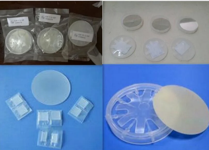
6. Pictures